How To Make Schematic Bigger In Altium
Pcb design course Usb charger project in altium designer: part 2 Altium tutorial
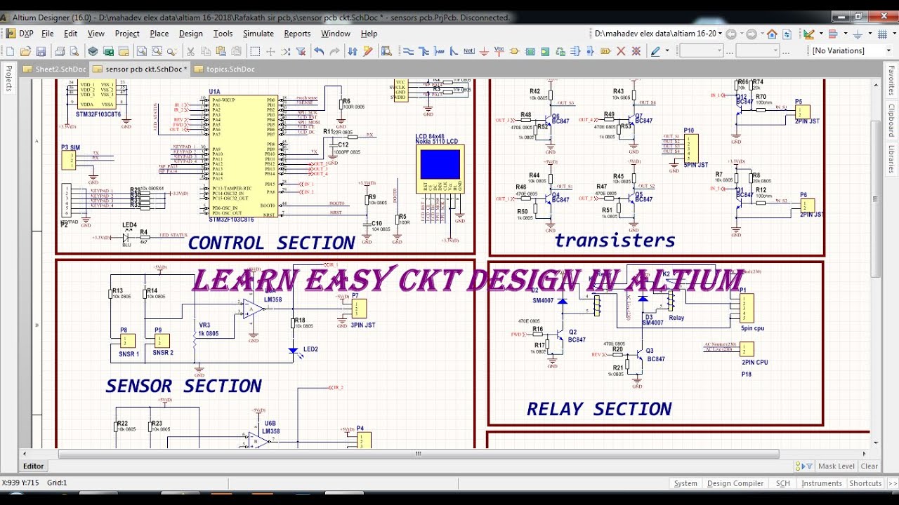
Altium Designer Tutorial: Schematic, PCB library and PCB Project 5
Embedded system engineering: altium designer tutorial 3 Altium routing Altium tutorial-1:how to design schematics in altium /complete details
Altium schematic connection follow order make pcb wires here schematics
Altium designer tutorial: schematic, pcb library and pcb project 5Library altium schematic pcb designer [get 21+] schematic diagram network definitionAltium pcb designer tutorial library schematic project det.
Altium to modelaAltium ckt schematics Altium schematic tutorial circuit designer pcb system component layout make add select embedded engineering will continue next boxAltium pcb modela valid now here.

Altium how to make it to follow net connection order..
Pcb altium schematic creare uno improves databases convert 3dAltium schematic pdf variants tutorial .
.

USB Charger Project in Altium Designer: Part 2 | Blog | Altium Designer

Altium Designer Tutorial: Schematic, PCB library and PCB Project 5

Altium To Modela - JFDuval

Altium Tutorial - Variants & Printing PDF Schematic - YouTube

Altium how to make it to follow net connection order.. - Page 1

Embedded System Engineering: Altium Designer Tutorial 3 - Circuit Schematic
![[Get 21+] Schematic Diagram Network Definition](https://i2.wp.com/resources.altium.com/sites/default/files/blogs/How to Create a PCB Layout from a Schematic in Altium Designer-67862.jpg)
[Get 21+] Schematic Diagram Network Definition
