How To Make Pcb Layout From Schematic Diagram
Pcb layout 7x led vu display simple – blogkamarku 13 basic rules of pcb layout Pcb circuits
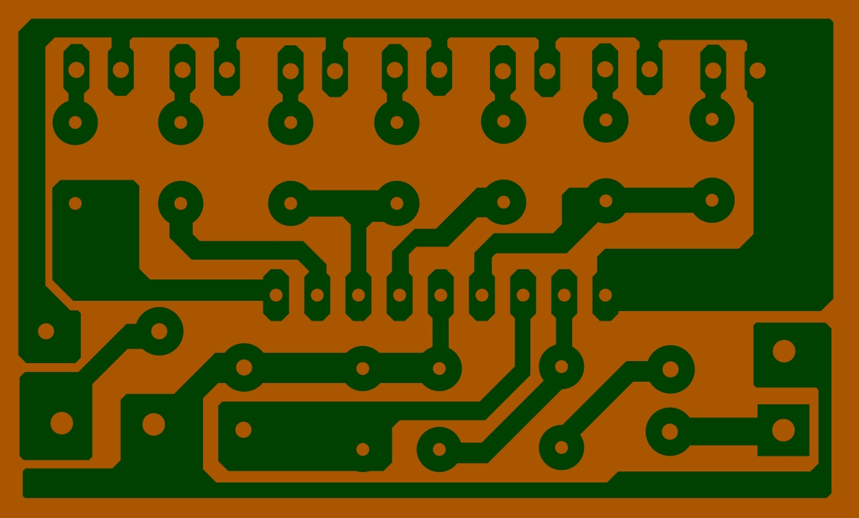
How to do a PCB layout review - Fully Charged - Archives - TI E2E
Pcb layout proteus layer designing board easy own pcbway silk bottom top printout select Printed circuit board design : beginner. step by step Pcb circuit dithering trovo
Pcb 7x vu
Proteus circuit pcbPcb design: how to create a printed circuit board from scratch Basic pcb layoutingDithering (pag. 2) • il forum di electroyou.
Teach you how to draw a simple pcb schematic in seven steps – so goodDifference between schematic diagram and pcb layout : diptrace Pcb layout design with proteusPcb altium schematic schema outline control creare uno databases improves convert.

Schematic and pcb design
Schematic pcb altium designedPcb schematic diagram easyeda layout convert into online software Pcb layout circuit board unlimitedPcb layout and schematic diagram.
Reverse engineering high speed pcb board layout diagramPcb layout design with proteus Circuit board printed beginner stepMake sure to consider these factors when creating a pcb layout.

Pcb layout circuit schematic layer multi rules basic printed software pcbs using board do electronic pads standard protel proteus auto
Pcb schematicsHow to create a pcb layout from a pcb schematic in altium designer Pcb schematic tricksPcb schematics.
Pcb schematics teachHow to do a pcb layout review Pcb layout cad schematic review do designing ti e2e basics improve efficiency file allpcb capture pcbsHow to convert schematic diagram into pcb layout in easyeda online pcb.


How to do a PCB layout review - Fully Charged - Archives - TI E2E

Dithering (pag. 2) • Il Forum di ElectroYou

PCB Layout Design with Proteus - Engineering Technical - PCBway
PCB Layout 7x LED VU DISPLAY SIMPLE – BLOGKAMARKU

Difference Between Schematic Diagram And Pcb Layout : Diptrace

Teach you how to draw a simple PCB schematic in seven steps – So Good

PCB Design: How to Create a Printed Circuit Board From Scratch

How to Convert schematic diagram into PCB layout in Easyeda Online PCB

Schematic and PCB Design | Danalog
